
Stránky farnosti sv. Matěje
Losovali tedy a los padl na Matěje - Sk 1,26


9. 3. 2026
13. březen: Den modlitby a půstu za mír
Arcibiskup olomoucký Mons. Josef Nuzík se jménem České biskupské konference připojuje k apelu papeže Lva XIV., který v souvislosti s eskalací konfliktu na Blízkém východě vyzval, aby „byla zastavena spirála násilí, než se stane nenapravitelnou propastí“, a vyhlašuje pátek 13. března Dnem modlitby a půstu za mír ve světě.
21. 2. 2026
Křížové cesty v době postní
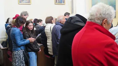
V postní době se vždy v pátek po mši svaté (cca 17h) koná pobožnost křížové cesty. Zveme všechny k účasti. Zároveň prosíme ty, kdo by byli ochotni křížovou cestu vést, aby se zapsali na seznam na nástěnce v kostele.
5. 2. 2026
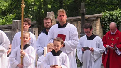
Plán pátečních bohoslužeb s promluvou pro děti
Harmonogram pátečních bohoslužeb s promluvou pro děti a dětských schůzek na 2. pololetí školního roku 2025/2026.
O farnosti
Kostel sv. Matěje
Objevte příběh kostela sv. Matěje, významné náboženské a kulturní stavby, jejíž počátky jsou v kronikách spojovány již s rokem 971.
Více o našem kostelu

Perníkové jesličky
Tradice svatomatějského perníkového betlému sahá až do roku 1972. Přečtěte si více o jeho historii a současnosti.
Více o perníkových jesličkách
